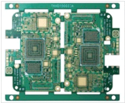
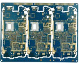
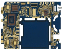
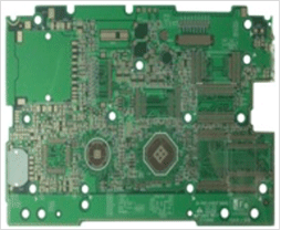
PCB Manufacture
who we are
Single Sided
Plated Through Hole
Multi-Layer (Up to 40 Layers) including buried and blind Via’s
Multi-Layer with bonded heat sinks
Flexible PCB
Flex-Rigid PCB
our advantage
High Temperature (Polyimide)
Microwave (PTFE)
Copper Invar Construction
Special Gold for ‘Chip on Board’
Controlled Impedance
Aluminium Clad Technologies
why choose us
Fast/Quick Turn PCB Prototyping
Good quality
DFM simulation


LINKYTECH TECHNOLOGY
Design、PCB FAB、SMT、Purchasing、Test 、Turn-key Solution
| PCB capability | ||
|---|---|---|
| Proto-typing | Mass-product | |
| Layer | 2-64L | 2-58L |
| Thickness | 0.5-17.5mm | 0.6-10mm |
| Min Mechanical | 0.1mm | 0.2mm |
| Min Laser Hole | 3mil | 4mil |
| HDI | 1+n+1\2+n+2\3+n+3 | 1+n+1\2+n+2\3+n+3 |
| Min Width/Space | 3/3mil | 3.5mil/3.5mi |
| Layer | 2-64L | 2-58L |
| thickness | 0.5-17.5mm | 0.6-10mm |
| Min Mechanical | 0.1mm | 0.2mm |
| Min Laser Hole | 3mil | 4mil |
| HDI | 1+n+1\2+n+2\3+n+3 | 1+n+1\2+n+2\3+n+3 |
| Min Width/Space | 3/3mil | 3.5mil/3.5mi |
| Lead Time | |||
|---|---|---|---|
| Layer | Mass production | Prototype | Quick Turn |
| 2L | 10days | 5days | 3days |
| 4L | 12days | 6days | 3days |
| 6L | 12days | 7days | 4days |
| 8L | 14days | 10days | 4days |
| 10L | 14days | 10days | 5days |
| 12L | 16days | 12days | 6days |
| 14L | 16days | 12days | 6days |
| 16L | 18days | 14days | 6days |
| 18L | 18days | 14days | 10days |
| 20L | 20days | 14days | 10days |
| 22L | 20days | 14days | 10days |
| 24L | 20days | 14days | 10days |
| 26L | 20days | 5days | 3days |
| This is the time after the confirmation of the project | |||
